Versal™ AI Edge Series Gen 2 – Inter-Processor Interrupt Buffer Peripheral Protection Unit Access Violation
Summary
The Versal™ AI Edge Series Gen 2 and Prime Series Gen 2 Peripheral Protection Unit (XPPU) for the inter-processor interrupt (IPI) message buffers and the IPI no-buffer control registers reports an access violation but does not correctly block the transaction. This is due to an issue in silicon where the latency of the security error, i.e. blocking the transaction, does not align with the transaction beat and is off by one cycle. For a detailed description of the Peripheral Protection Units, please refer to Versal AI Edge Series Gen 2 and Prime Series Gen 2 Technical Reference Manual Peripheral Protection Units chapter (AM026 – Peripheral Protection Units).
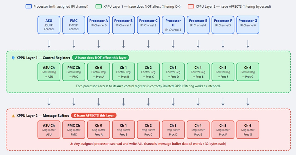
The IPI architecture of the Adaptive SoC is designed in such a manner to provide communication between different processors within the SoC. In the case of IPI communication with a dedicated message buffer there are a total of seven (7) IPI channels that can be assigned to the various processors within the Adaptive SoC as well as two (2) assigned channels for the Platform Management Controller (PMC) and Application Security Unit (ASU) for a total of nine (9) IPI channels with dedicated message buffers. To start the communication process, a source processor sends an inter-processor interrupt to a destination processor. The destination processor receives the interrupt and reads the 8 words, 32 bytes total, located in its dedicated IPI channel’s message buffer. Note that the ASU firmware only uses the ASU IPI interrupts with a dedicated memory mailbox to exchange information with remote processors – the ASU does not use the IPI message buffers. Refer to the Security Libraries Reference Guide (UG1540) for additional information regarding the IPI communication architecture as well as the ASU firmware architecture.
For IPI communications with a dedicated message buffer, there are two layers of XPPU protection. The first layer of XPPU isolation is for the control registers dedicated to each of the nine (9) IPI channels, which this issue does not affect, and a second layer of XPPU isolation for protecting each IPI Channel’s message buffer, which this issue affects. Any processor that has a channel assigned in the IPI message buffer will be allowed to read and write all the other channels’ message buffer data. Please see the following figure for a summary of this issue as related to the IPI communications with a dedicated message buffer.
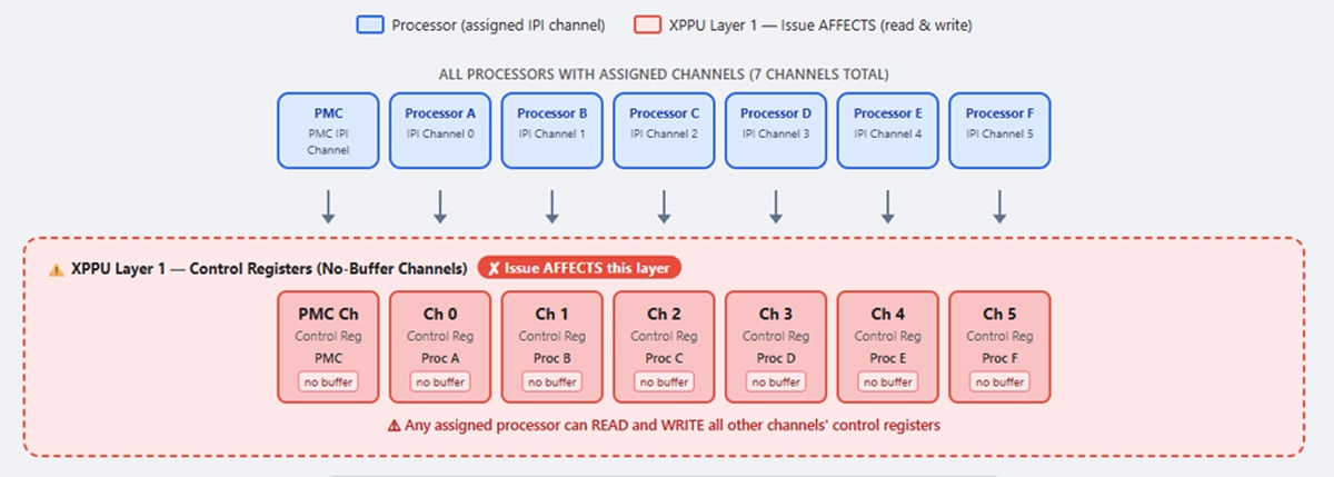
In the case of IPI communications without a dedicated message buffer (channels with the suffix _NOBUF, _NOBUFF, or _NB), only an inter-processor interrupt is sent by a source processor and received by the destination processor with a total seven (7) channels compared to nine (9) channels as above. The customer’s system architecture determines how the destination processor handles the interrupt. For example, a dedicated location of memory could be used as a communication mailbox in which the size is defined by the customer and is read when a destination interrupt is received. In other cases, the destination interrupt could trigger application specific functionality such as loading of a new image or trigger specific functionality within the programmable logic (PL). This issue affects the control registers for the IPI no-buffer channels such that any processor that has a channel assigned would be able to read and write all the other channel’s control registers. This issue is shown in the following figure.
CVE Details
Refer to Glossary for explanation of terms
CVE |
CVE Description |
CVSS Score |
CVE-2026-0455 |
The Versal™ AI Edge Series Gen 2 Peripheral Protection Unit (XPPU) for the inter-processor interrupt (IPI) buffers does not block unauthorized access as expected. This allows processors in the SoC with any IPI channel access the ability to both read and write to the entire IPI buffer register space as well as the IPI no-buffer register control space. |
5.9 (Medium) CVSS:4.0/AV:L/AC:L/AT:P/PR:L/UI:A/VC:L/VI:L/VA:H/SC:L/SI:L/SA:H |
Specific CVSS scores may change subject to your implementation. We encourage you to calculate CVSS scores independently for your system.
Affected Products and Mitigation
AMD recommends implementing the mitigated version indicated below.
A software mitigation will configure by default the global Inter-Processor Interrupt (IPI) Peripheral Protection Unit (XPPU) to trigger a soft reset (SRST) of any processor making a channel access violation to the IPI buffer registers or the IPI no-buffer control registers. Other responses are allowed to be configured in the Advanced Configuration Editor (ACE), see the ACE User Guide (UG1650), but are not as secure as the recommended AMD setting.
Product |
Mitigation |
Mitigation Release Date |
Vivado Advanced Configuration Editor for Versal AI Edge Series Gen 2 |
2026.1 |
2026-06-23 |
| Versal™ AI Edge Series Gen 2 Adaptive SoCs | 2026.1 | 2026-06-23 |
| Versal™ Prime Series Gen 2 Adaptive SoCs | 2026.1 | 2026-06-23 |
References
Acknowledgement
Internally reported
Revisions
| Revision Date | Description |
| 2026-11-10 | Initial version |
DISCLAIMER
The information contained herein is for informational purposes only and is subject to change without notice. While every precaution has been taken in the preparation of this document, it may contain technical inaccuracies, omissions and typographical errors, and AMD is under no obligation to update or otherwise correct this information. Advanced Micro Devices, Inc. makes no representations or warranties with respect to the accuracy or completeness of the contents of this document, and assumes no liability of any kind, including the implied warranties of noninfringement, merchantability or fitness for particular purposes, with respect to the operation or use of AMD hardware, software or other products described herein. Any computer system has risks of security vulnerabilities that cannot be completely prevented or mitigated. No license, including implied or arising by estoppel, to any intellectual property rights is granted by this document. Terms and limitations applicable to the purchase or use of AMD’s products are as set forth in a signed agreement between the parties or in AMD's Standard Terms and Conditions of Sale.
AMD, the AMD Arrow logo, Versal, and combinations thereof are trademarks of Advanced Micro Devices, Inc. CVE and the CVE logo are registered trademarks of The MITRE Corporation. Other product names used in this publication are for identification purposes only and may be trademarks of their respective companies.
Third party content may be licensed to you directly by the third party that owns the content and is not licensed to you by AMD. ALL LINKED THIRD-PARTY CONTENT IS PROVIDED ‘AS IS’ WITHOUT A WARRANTY OF ANY KIND. USE OF SUCH THIRD-PARTY CONTENT IS DONE AT YOUR SOLE DISCRETION AND UNDER NO CIRCUMSTANCES WILL AMD BE LIABLE TO YOU FOR ANY THIRD PARTY CONTENT. YOU ASSUME ALL RISK AND ARE SOLELY RESPONSIBILITY FOR ANY DAMAGES THAT MAY ARISE FROM YOUR USE OF THIRD-PARTY CONTENT.
© 2026 Advanced Micro Devices, Inc. All rights reserved.