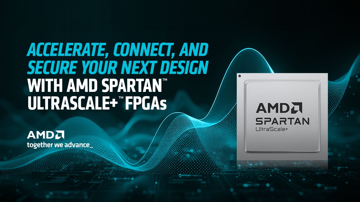
Accelerate, Connect, and Secure Your Next Design with Spartan™ UltraScale+™ FPGAs
Dec 02, 2025
At a Glance
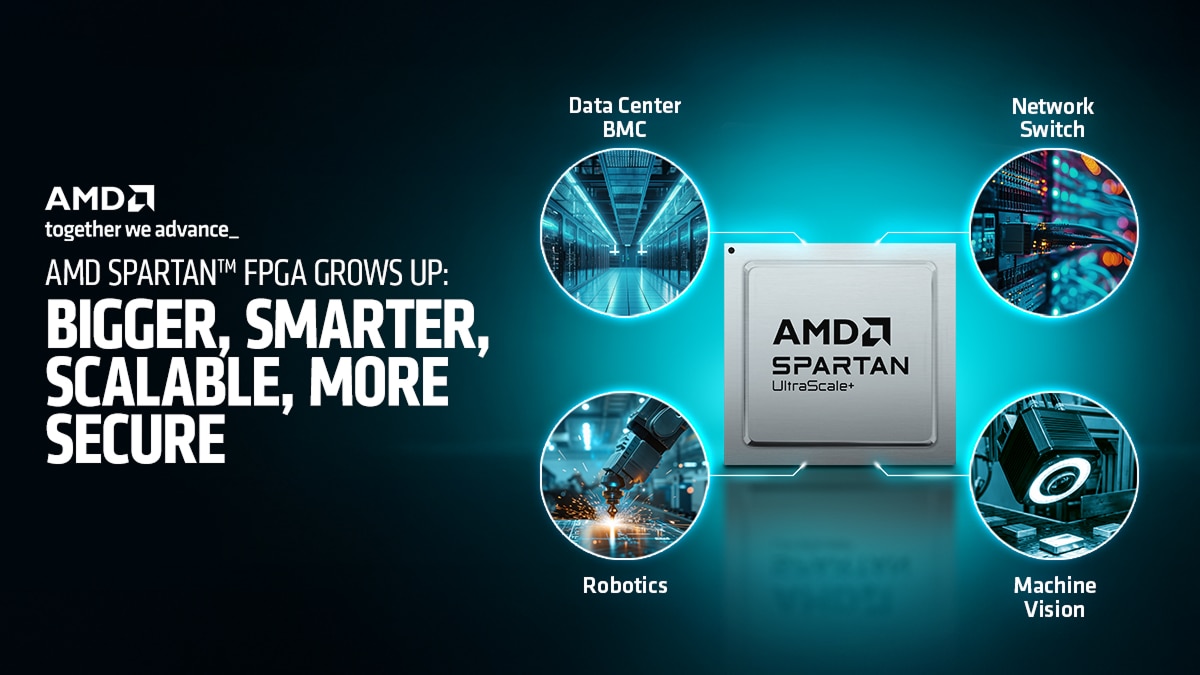
In industrial automation and wired networking systems, designers face mounting challenges finding the right cost-effective solution that balances high-speed data transfer, flexible I/O integration, and long product lifecycles, while maintaining power efficiency and security. To address these growing market needs, AMD introduces two new members of the AMD Spartan™ UltraScale+™ FPGA family, the SU45P and SU60P, which are the smallest devices in the family featuring fast transceivers and PCIe® Gen4 connectivity. This enhanced connectivity, combined with the Spartan UltraScale+ FPGA’s advanced security features, provides a compact, power-efficient architecture enabling fast, reliable industrial and wired system designs.
Cost-Optimized FPGAs for Long-Term Design Success
Feature rich, built on a 16 nm FinFET node, the Spartan UltraScale+ devices offer:
- Compact, low-power architecture, reducing thermal management in a space-constrained environment, ideal for control-plane and line-card designs
- AMD Vivado™ Design Suite, a unified design flow achieving superior timing and routing closure vs. competing solutions, reducing development efforts, improving design cycle and time to market1
- Stable long-term supply to reduce costly redesign and requalification cycles with a footprint compatibility upgrade path from Spartan UltraScale+ SU10P/SU25P/SU35P FPGAs
High-Speed Interfaces and I/O Diversity for Seamless Integration
Spartan UltraScale+ FPGAs enable fast, flexible connectivity for modern industrial and networking designs that demand seamless and reliable data movement
- Enable high-speed connectivity through 16.3G transceivers and PCIe® Gen4 interfaces, delivering fast data transfer and low latency for machine vision and networking systems
- Support mixed-voltage I/Os including 3.3V and lower-voltage standards, allowing easy integration of both legacy and high-speed I/Os on a single device
- Simplify system integration and accelerate design cycles by allowing engineers to seamlessly connect and synchronize diverse sensors, optical modules, and control interfaces
Security You Can Trust
Security and firmware integrity are now more important than ever in network and industrial control systems.
Spartan UltraScale+ FPGAs integrate:
- CNSA 2.0–Compliant Secure Boot: Hardware root-of-trust with PQC-ready LMS algorithms helps ensure firmware authenticity and protection against tampering
- Robust Data Integrity: AES-GCM-256 encryption with DPA-protected key handling to prevent cloning and unauthorized access
- Lifecycle Protection: Device control through family key-based authentication, simplifying field updates and long-term product security
Competitive Advantages
Feature |
AMD Spartan UltraScale+ SU45P/SU60P |
Lattice MachXO5-NX LFMXO5-65T |
Altera Agilex 3 A3C100 |
Transceiver Speed |
16.3 Gb/s |
10.3 Gb/s |
12.5 Gb/s |
Total Transceiver Bandwidth |
65.2 Gb/s |
20.6 Gb/s |
50.0 Gb/s |
PCIe Generation |
Gen 4 |
Gen 2 |
Gen 3 |
Total PCIe Bandwidth |
63.0 Gb/s |
8.0 Gb/s |
31.5 Gb/s |
Results:
- Up to 3.2X more transceiver bandwidth and 1.6X faster lanes vs. the competition2
- Up to 1.3X higher transceiver bandwidth and 1.3X faster lanes vs. the competition3
- Up to 2X-8X higher PCIe bandwidth vs. the competition4,5
- Up to 40% better LUT utilization with LUT6 vs. LUT4 competitive vendors6
- Up to 1.8X greater FMAX enables selection of lowest possible speed grade vs. competitive vendors7
Learn more about how Spartan UltraScale+ FPGAs can accelerate your next-generation designs
AMD Spartan UltraScale+ SU45P and SU60P FPGAs address core challenges of modern industrial and networking systems by delivering high-speed connectivity, robust security, and long-term reliability in power-efficient, cost-optimized FPGAs. Learn more about Spartan UltraScale+ FPGAs.
Spartan UltraScale+ SU45P and SU60P FPGAs will have early access Vivado tool support in 1H’26 with silicon availability in 2H’26. Contact your local FAE to learn more and request early access.
Footnotes
*No technology or product can be completely secure.
- Based on AMD place-and-route testing in September 2024, using 26 open-core designs compiled with Vivado 2024.1 and Lattice Radiant Software 2024.1 in default mode, with the Artix UltraScale+ AU10P device versus Lattice Mach LFMXO5 device @ 150 MHz FMAX target; and Kintex UltraScale+ KU5P device versus Lattice Avant E70 device @ 200 MHz FMAX target. P&R performance will vary based on device, design, configuration, and other factors. (VIV-014)
- Based on AMD internal comparison in October 2025 on the AMD Spartan UltraScale+ SU60P FPGA with four (4) transceivers running at 16.3 GB/s versus Lattice MachXO5 LFMXO5-65T FPGA with two (2) transceivers, at 10.3 GB/s, to calculate the total transceiver bandwidth and per-lane speeds for each device. For the publicly available competitive specs, see: https://www.latticesemi.com/en/Products/FPGAandCPLD/MachXO5-NX. AMD specs based on internal engineering documentation. Device manufacturers may vary specifications, yielding different results. Results may vary. (SUS-017)
- Based on AMD internal comparison in October 2025 of an AMD Spartan UltraScale+ SU60P FPGA with four (4) transceivers running at 16.3 GB/s versus Altera Agilex 3 A3C100 FPGA with four (4) transceivers at 12.5 GB/s, to calculate the total transceiver bandwidth and per-lane speeds for each device. For the publicly available competitive specs, see: https://www.altera.com/products/fpga/agilex/3. AMD specs based on internal engineering documentation. Device manufacturers may vary specifications, yielding different results. Results may vary. (SUS-018)
- Based on AMD internal comparison in October 2025 of an AMD Spartan UltraScale+ SU60P FPGA with PCIe Gen4 x4 versus Lattice MachXO5 LFMXO5-65T FPGA with PCIe Gen2 x2 lanes, to calculate the PCIe bandwidth for each device. For the publicly available competitive specs, see: https://www.latticesemi.com/en/Products/FPGAandCPLD/MachXO5https://www.altera.com/products/fpga/agilex/3. AMD specs based on internal engineering documentation. Device manufacturers may vary specifications, yielding different results. Results may vary. (SUS-019)
- Based on AMD internal comparison in October 2025 of an AMD Spartan UltraScale+ SU60P FPGA with PCIe Gen4 x4 lanes versus Altera Agilex 3 A3C100 FPGA with PCIe Gen3 x4 lanes, to calculate the PCIe bandwidth for each device. For the publicly available competitive specs, see: https://www.altera.com/products/fpga/agilex/3. AMD specs based on internal engineering documentation. Device manufacturers may vary specifications, yielding different results. Results may vary. (SUS-020)
- Based on AMD testing in July 2024, measuring the utilization scores of the LUT6 architecture-based AMD Artix 7 A100T (28 nm) and Artix UltraScale+ AU7P (16 nm) versus the LUT4 architecture-based Lattice Nexus MachXO5 25 (28 nm) and Lattice Avant E70 (16 nm) devices, measured on AMD Vivado™ 2024.1 and Lattice Radiant 2024.1, respectively, at various speed grades, averaged over 30 open-core designs. Results will vary based on architecture, device, speed grade, package size, design, configuration, and other factors. (COP-001)
- Based on AMD analysis in July 2024, calculating FMAX ratios averaged over 30 open-core designs for (16 nm) AMD Artix UltraScale+ AU7P FPGA, compared to the (16 nm) Lattice Avant E70 FPGA, at the respective highest speed grades. Results will vary based on architecture, device, speed grade, package size, design, configuration, and other factors. (AUS-010)

Related Blogs
-
Efficient Hyperparameter Optimization for Autonomous Driving Models with AMD Instinct GPU Partitioning — ROCm Blogs
Accelerate HPO for autonomous driving models using AMD MI300X GPU partitioning for higher throughput, efficiency, and parallelism.
July 07, 2026
-
AMD Ryzen™ AI Halo Now Available at Micro Center
Ryzen AI Halo launches at Micro Center, powering agentic PCs for developers building larger, next-generation local AI applications.
July 06, 2026
-
AMD Versal Premium Gen 2 MoP Boosts Memory Capacity
Explore AMD Versal Premium Gen 2 MoP, integrating up to 32GB LPDDR5X to boost bandwidth, reduce board area and accelerate design cycles.
June 30, 2026
-
MXFP6 and MXFP4 Mixed Precision for Accelerating Dense LLMs on AMD Instinct MI355X — ROCm Blogs
W_MXFP4_A_MXFP6 quantization on AMD Instinct MI355X improves LLM throughput and latency while recovering accuracy versus MXFP4.
June 25, 2026
-
AMD Named Current Company to Beat in Gartner® AI Vendor Race
In a new report, Gartner positions AMD as the current front-runner for enterprise AI server CPUs.
June 24, 2026
-
A Practical Guide to Running LLMs on AMD Radeon™ GPUs — ROCm Blogs
This guide describes how to run LLMs on AMD Radeon™ GPUs using a range of partner frameworks, tools, and runtimes, with step-by-step setup instructions and performance optimization tips.
June 18, 2026
-
AI Across Industries: How AMD Technologies Are Powering the Next Wave of Enterprise Transformation
AI is reshaping every industry. Explore how leading enterprises are using AMD-powered AI infrastructure to accelerate innovation, improve efficiency, and drive business transformation.
June 18, 2026
-
AMD Spartan™ UltraScale+™ SU200P FPGA Now in Production
Now in production. AMD Spartan™ UltraScale+™ SU200P FPGA with high I/O, low power, and state-of-the-art security features.
June 15, 2026