

Supercharging AI and HPC
AMD Instinct™ MI300 Series accelerators are uniquely well-suited to power even the most demanding AI and HPC workloads, offering exceptional compute performance, large memory density with high bandwidth, and support for specialized data formats.
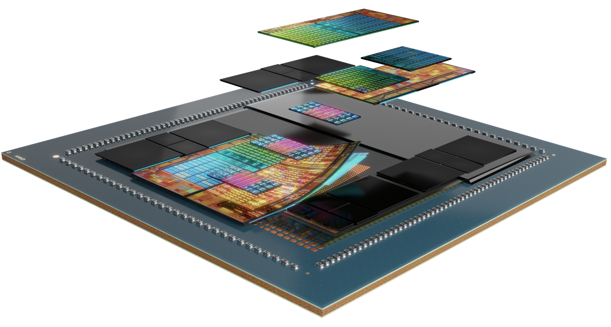
Under the Hood
AMD Instinct MI300 Series accelerators are built on AMD CDNA™ 3 architecture, which offers Matrix Core Technologies and support for a broad range of precision capabilities—from the highly efficient INT8 and FP8 (including sparsity support for AI), to the most demanding FP64 for HPC.

Meet the Series
Explore AMD Instinct MI300 Series accelerators, AMD Instinct MI300 Series Platforms, and AMD Instinct MI300A APU.

Meet the AMD Instinct™ MI325X Accelerators
The AMD Instinct™ MI325X GPU accelerator sets new standards in AI performance with 3rd Gen AMD CDNA™ architecture, delivering incredible performance and efficiency for training and inference. With industry leading 256 GB HBM3E memory and 6 TB/s bandwidth, they optimize performance and help reduce TCO.1
304 CUs
304 GPU Compute Units
256 GB
256 GB HBM3E Memory
6 TB/s
6 TB/s Peak Theoretical Memory Bandwidth
Specs Comparisons
- AI Performance
- HPC Performance
- Memory
AI Performance (Peak TFLOPs)
Up to 1.3X the AI performance vs. competitive accelerators2, 3
TF32
FP16/BF16 (Tensor/Matrix)
FP8
H200 SXM 141 GB
MI325X OAM 256 GB
HPC Performance (Peak TFLOPs)
Up to 2.4X the HPC performance vs. competitive accelerators3
FP64 (Vector)
FP64 (Tensor / Matrix)
FP32 (Vector)
H200 SXM 141 GB
MI325X OAM 256 GB
Memory Capacity & Bandwidth
1.8X Memory Capacity and 1.2X Memory Bandwidth vs. competitive accelerators1
Memory Capacity
Memory Bandwidth
H200 SXM 141 GB
MI325X OAM 256 GB

Instinct MI300X Accelerators
AMD Instinct MI300X Series accelerators are designed to deliver leadership performance for Generative AI workloads and HPC applications.
304 CUs
304 GPU Compute Units
192 GB
192 GB HBM3 Memory
5.3 TB/s
5.3 TB/s Peak Theoretical Memory Bandwidth
AI Performance (Peak TFLOPs)
Up to 1.3X the AI performance vs. competitive accelerators6
TF32 (Sparsity)
FP16/BF16 (Sparsity)
FP8 (Sparsity)
HPC Performance (Peak TFLOPs)
Up to 2.4X the HPC performance vs. competitive accelerators7
FP64 (Vector)
FP64 (Tensor / Matrix)
FP32 (Vector)
Memory Capacity & Bandwidth
2.4X Memory Capacity and 1.6X Peak Theoretical Memory Bandwidth vs. competitive accelerators8
Memory Capacity
Memory Bandwidth

AMD Instinct Platforms
The AMD Instinct MI325X Platform integrates 8 fully connected MI325X GPU OAM modules onto an industry-standard OCP design via 4th-Gen AMD Infinity Fabric™ links, delivering up to 2TB HBM3E capacity for low-latency AI processing. This ready-to-deploy platform can accelerate time-to-market and reduce development costs when adding MI325X accelerators into existing AI rack and server infrastructure.
8 MI325X
8 MI325X GPU OAM modules
2 TB
2 TB Total HBM3E Memory
48 TB/s
48 TB/s Peak Theoretical Aggregate Memory Bandwidth

AMD Instinct MI300A APUs
AMD Instinct MI300A accelerated processing units (APUs) combine the power of AMD Instinct accelerators and AMD EPYC™ processors with shared memory to enable enhanced efficiency, flexibility, and programmability. They are designed to accelerate the convergence of AI and HPC, helping advance research and propel new discoveries.
228 CUs
228 GPU Compute Units
24
24 “Zen 4” x86 CPU Cores
128 GB
128 GB Unified HBM3 Memory
5.3 TB/s
5.3 TB/s Peak Theoretical Memory Bandwidth
AI Performance (Peak TFLOPs)11
TF32 (Sparsity)
FP16/BF16 (Sparsity)
FP8 (Sparsity)
HPC Performance (Peak TFLOPs)
Up to 1.8X the HPC performance vs. competitive accelerators12
FP64 (Vector)
FP64 (Tensor / Matrix)
FP32 (Vector)
Memory Capacity & Bandwidth
2.4X Memory Capacity and 1.6X Peak Theoretical Memory Bandwidth vs. competitive accelerators13
Memory Capacity
Memory Bandwidth
Advancing Exascale Computing
AMD Instinct accelerators power some of the world’s top supercomputers, including Lawrence Livermore National Laboratory’s El Capitan system. See how this two-Exascale supercomputer will use AI to run first-of-its-kind simulations and advance scientific research.

AMD ROCm™ Software
AMD ROCm™ software includes a broad set of programming models, tools, compilers, libraries, and runtimes for AI models and HPC workloads targeting AMD Instinct accelerators.
Case Studies
-
AT&T Achieves Outstanding Efficiency for AI Training with AMD
AT&T trains telecom AI on AMD Instinct™ MI355X GPUs, running a full model on a single GPU to power inference for millions of customers.
July 02, 2026
-
UNISON’s Yuca Supercomputer Powered by AMD Accelerates Science
University of Sonora builds the highest performing research supercomputing cluster in Mexico, powered by Dell PowerEdge XE-Series Servers with AMD EPY…
May 26, 2026
-
TensorWave: Reliable, Resilient, Cost-Optimized AI Cloud
TensorWave built an AMD Instinct™ GPU cloud delivering reliable, resilient AI infrastructure with up to 2x performance and 40–60% cost savings vs. alt…
May 06, 2026
-
Maincode Builds An AI Factory for Australia with AMD
Maincode’s upcoming $30M MC-2 AI factory uses AMD Instinct™ MI355X GPUs to deliver sovereign, cost-efficient AI systems for Australian enterprises.
April 16, 2026


Find Solutions
Find a partner offering AMD Instinct accelerator-based solutions.


Resources

Stay Informed
Sign up to receive the latest data center news and server content.
Footnotes
- MI325-001A - Calculations conducted by AMD Performance Labs as of September 26th, 2024, based on current specifications and /or estimation. The AMD Instinct™ MI325X OAM accelerator will have 256GB HBM3E memory capacity and 6 TB/s GPU peak theoretical memory bandwidth performance. Actual results based on production silicon may vary.
The highest published results on the NVidia Hopper H200 (141GB) SXM GPU accelerator resulted in 141GB HBM3E memory capacity and 4.8 TB/s GPU memory bandwidth performance. https://nvdam.widen.net/s/nb5zzzsjdf/hpc-datasheet-sc23-h200-datasheet-3002446
The highest published results on the NVidia Blackwell HGX B100 (192GB) 700W GPU accelerator resulted in 192GB HBM3E memory capacity and 8 TB/s GPU memory bandwidth performance.
The highest published results on the NVidia Blackwell HGX B200 (192GB) GPU accelerator resulted in 192GB HBM3E memory capacity and 8 TB/s GPU memory bandwidth performance.
Nvidia Blackwell specifications at https://resources.nvidia.com/en-us-blackwell-architecture?_gl=1*1r4pme7*_gcl_aw*R0NMLjE3MTM5NjQ3NTAuQ2p3S0NBancyNkt4QmhCREVpd0F1NktYdDlweXY1dlUtaHNKNmhPdHM4UVdPSlM3dFdQaE40WkI4THZBaWFVajFy
- MI325-002 - Calculations conducted by AMD Performance Labs as of May 28th, 2024 for the AMD Instinct™ MI325X GPU resulted in 1307.4 TFLOPS peak theoretical half precision (FP16), 1307.4 TFLOPS peak theoretical Bfloat16 format precision (BF16), 2614.9 TFLOPS peak theoretical 8-bit precision (FP8), 2614.9 TOPs INT8 floating-point performance. Actual performance will vary based on final specifications and system configuration.
Published results on Nvidia H200 SXM (141GB) GPU: 989.4 TFLOPS peak theoretical half precision tensor (FP16 Tensor), 989.4 TFLOPS peak theoretical Bfloat16 tensor format precision (BF16 Tensor), 1,978.9 TFLOPS peak theoretical 8-bit precision (FP8), 1,978.9 TOPs peak theoretical INT8 floating-point performance. BFLOAT16 Tensor Core, FP16 Tensor Core, FP8 Tensor Core and INT8 Tensor Core performance were published by Nvidia using sparsity; for the purposes of comparison, AMD converted these numbers to non-sparsity/dense by dividing by 2, and these numbers appear above
Nvidia H200 source: https://nvdam.widen.net/s/nb5zzzsjdf/hpc-datasheet-sc23-h200-datasheet-3002446 and https://www.anandtech.com/show/21136/nvidia-at-sc23-h200-accelerator-with-hbm3e-and-jupiter-supercomputer-for-2024
Note: Nvidia H200 GPUs have the same published FLOPs performance as H100 products https://resources.nvidia.com/en-us-tensor-core/. MI325-02
- MI325-008 - Calculations conducted by AMD Performance Labs as of October 2nd, 2024 for the AMD Instinct™ MI325X (1000W) GPU designed with AMD CDNA™ 3 5nm | 6nm FinFET process technology at 2,100 MHz peak boost engine clock resulted in 163.4 TFLOPs peak theoretical double precision Matrix (FP64 Matrix), 81.7 TFLOPs peak theoretical double precision (FP64), 163.4 TFLOPs peak theoretical single precision Matrix (FP32 Matrix), 163.4 TFLOPs peak theoretical single precision (FP32), 653.7 TFLOPS peak theoretical TensorFloat-32 (TF32), 1307.4 TFLOPS peak theoretical half precision (FP16), Actual performance may vary based on final specifications and system configuration.
Published results on Nvidia H200 SXM (141GB) GPU: 66.9 TFLOPs peak theoretical double precision tensor (FP64 Tensor), 33.5 TFLOPs peak theoretical double precision (FP64), 66.9 TFLOPs peak theoretical single precision (FP32), 494.7 TFLOPs peak TensorFloat-32 (TF32), 989.5 TFLOPS peak theoretical half precision tensor (FP16 Tensor). TF32 Tensor Core performance were published by Nvidia using sparsity; for the purposes of comparison, AMD converted these numbers to non-sparsity/dense by dividing by 2, and this number appears above.
Nvidia H200 source: https://nvdam.widen.net/s/nb5zzzsjdf/hpc-datasheet-sc23-h200-datasheet-3002446 and https://www.anandtech.com/show/21136/nvidia-at-sc23-h200-accelerator-with-hbm3e-and-jupiter-supercomputer-for-2024
Note: Nvidia H200 GPUs have the same published FLOPs performance as H100 products https://resources.nvidia.com/en-us-tensor-core/.
*Nvidia H200 GPUs don’t support FP32 Tensor.
- Measurements conducted by AMD Performance Labs as of November 11th, 2023 on the AMD Instinct™ MI300X (750W) GPU designed with AMD CDNA™ 3 5nm | 6nm FinFET process technology at 2,100 MHz peak boost engine clock resulted in 653.7 TFLOPS peak theoretical TensorFloat-32 (TF32), 1307.4 TFLOPS peak theoretical half precision (FP16), 1307.4 TFLOPS peak theoretical Bfloat16 format precision (BF16), 2614.9 TFLOPS peak theoretical 8-bit precision (FP8), 2614.9 TOPs INT8 floating-point performance. The MI300X is expected to be able to take advantage of fine-grained structure sparsity providing an estimated 2x improvement in math efficiency resulting 1,307.4 TFLOPS peak theoretical TensorFloat-32 (TF32), 2,614.9 TFLOPS peak theoretical half precision (FP16), 2,614.9 TFLOPS peak theoretical Bfloat16 format precision (BF16), 5,229.8 TFLOPS peak theoretical 8-bit precision (FP8), 5,229.8 TOPs INT8 floating-point performance with sparsity. The results calculated for the AMD Instinct™ MI250X (560W) 128GB HBM2e OAM accelerator designed with AMD CDNA™ 2 5nm FinFET process technology at 1,700 MHz peak boost engine clock resulted in TF32* (N/A), 383.0 TFLOPS peak theoretical half precision (FP16), 383.0 TFLOPS peak theoretical Bfloat16 format precision (BF16), FP8* (N/A), 383.0 TOPs INT8 floating-point performance. *AMD Instinct MI200 Series GPUs don’t support TF32, FP8 or sparsity. MI300-16
- Measurements by internal AMD Performance Labs as of June 2, 2023 on current specifications and/or internal engineering calculations. Large Language Model (LLM) run or calculated with FP16 precision to determine the minimum number of GPUs needed to run the Falcon-7B (7B, 40B parameters), LLaMA (13B, 33B parameters), OPT (66B parameters), GPT-3 (175B parameters), BLOOM (176B parameter), and PaLM (340B, 540B parameters) models. Calculated estimates based on GPU-only memory size versus memory required by the model at defined parameters plus 10% overhead. Calculations rely on published and sometimes preliminary model memory sizes. GPT-3, BLOOM, and PaML results estimated on MI300X due to system/part availability. Tested result configurations: AMD Lab system consisting of 1x EPYC 9654 (96-core) CPU with 1x AMD Instinct™ MI300X (192GB HBM3, OAM Module) 750W accelerator
Results (FP16 precision):
Model
Parameters
Tot Memory Reqd
MI300X Required
Falcon-7B
7 Billion
15.4 GB
1 Actual
LLaMA
13 Billion
44 GB
1 Actual
LLaMA
33 Billion
72.5 GB
1 Actual
Falcon-40B
40 Billion
88 GB
1 Actual
OPT
66 Billion
145.2 GB
1 Actual
GPT-3
175 Billion
385 GB
3 Calculated
Bloom
176 Billion
387.2 GB
3 Calculated
PaLM
340 Billion
748 GB
4 Calculated
PaLM
540 Billion
1188 GB
7 Calculated
Calculated estimates may vary based on final model size; actual and estimates may vary due to actual overhead required and using system memory beyond that of the GPU. Server manufacturers may vary configuration offerings yielding different results. MI300-07
- Measurements conducted by AMD Performance Labs as of November 11th, 2023 on the AMD Instinct™ MI300X (750W) GPU designed with AMD CDNA™ 3 5nm | 6nm FinFET process technology at 2,100 MHz peak boost engine clock resulted in 653.7 TFLOPS peak theoretical TensorFloat-32 (TF32), 1307.4 TFLOPS peak theoretical half precision (FP16), 1307.4 TFLOPS peak theoretical Bfloat16 format precision (BF16), 2614.9 TFLOPS peak theoretical 8-bit precision (FP8), 2614.9 TOPs INT8 floating-point performance. The MI300X is expected to be able to take advantage of fine-grained structure sparsity providing an estimated 2x improvement in math efficiency resulting 1,307.4 TFLOPS peak theoretical TensorFloat-32 (TF32), 2,614.9 TFLOPS peak theoretical half precision (FP16), 2,614.9 TFLOPS peak theoretical Bfloat16 format precision (BF16), 5,229.8 TFLOPS peak theoretical 8-bit precision (FP8), 5,229.8 TOPs INT8 floating-point performance with sparsity. Published results on Nvidia H100 SXM (80GB) 700W GPU resulted in 989.4 TFLOPs peak TensorFloat-32 (TF32) with sparsity, 1,978.9 TFLOPS peak theoretical half precision (FP16) with sparsity, 1,978.9 TFLOPS peak theoretical Bfloat16 format precision (BF16) with sparsity, 3,957.8 TFLOPS peak theoretical 8-bit precision (FP8) with sparsity, 3,957.8 TOPs peak theoretical INT8 with sparsity floating-point performance. Nvidia H100 source: https://resources.nvidia.com/en-us-tensor-core. MI300-17
- Measurements conducted by AMD Performance Labs as of November 11th, 2023 on the AMD Instinct™ MI300X (750W) GPU designed with AMD CDNA™ 3 5nm | 6nm FinFET process technology at 2,100 MHz peak boost engine clock resulted in 163.4 TFLOPs peak theoretical double precision Matrix (FP64 Matrix), 81.7 TFLOPs peak theoretical double precision (FP64), 163.4 TFLOPs peak theoretical single precision Matrix (FP32 Matrix), 163.4 TFLOPs peak theoretical single precision (FP32), 653.7 TFLOPS peak theoretical TensorFloat-32 (TF32), 1307.4 TFLOPS peak theoretical half precision (FP16), 1307.4 TFLOPS peak theoretical Bfloat16 format precision (BF16), 2614.9 TFLOPS peak theoretical 8-bit precision (FP8), 2614.9 TOPs INT8 floating-point performance. Published results on Nvidia H100 SXM (80GB) GPU resulted in 66.9 TFLOPs peak theoretical double precision tensor (FP64 Tensor), 33.5 TFLOPs peak theoretical double precision (FP64), 66.9 TFLOPs peak theoretical single precision (FP32), 494.7 TFLOPs peak TensorFloat-32 (TF32)*, 989.4 TFLOPS peak theoretical half precision tensor (FP16 Tensor), 133.8 TFLOPS peak theoretical half precision (FP16), 989.4 TFLOPS peak theoretical Bfloat16 tensor format precision (BF16 Tensor), 133.8 TFLOPS peak theoretical Bfloat16 format precision (BF16), 1,978.9 TFLOPS peak theoretical 8-bit precision (FP8), 1,978.9 TOPs peak theoretical INT8 floating-point performance. Nvidia H100 source: https://resources.nvidia.com/en-us-tensor-core/ * Nvidia H100 GPUs don’t support FP32 Tensor. MI300-18
- Calculations conducted by AMD Performance Labs as of November 17, 2023, for the AMD Instinct™ MI300X OAM accelerator 750W (192 GB HBM3) designed with AMD CDNA™ 3 5nm FinFet process technology resulted in 192 GB HBM3 memory capacity and 5.325 TFLOPS peak theoretical memory bandwidth performance. MI300X memory bus interface is 8,192 and memory data rate is 5.2 Gbps for total peak memory bandwidth of 5.325 TB/s (8,192 bits memory bus interface * 5.2 Gbps memory data rate/8). The highest published results on the NVidia Hopper H200 (141GB) SXM GPU accelerator resulted in 141GB HBM3e memory capacity and 4.8 TB/s GPU memory bandwidth performance. https://nvdam.widen.net/s/nb5zzzsjdf/hpc-datasheet-sc23-h200-datasheet-3002446 The highest published results on the NVidia Hopper H100 (80GB) SXM5 GPU accelerator resulted in 80GB HBM3 memory capacity and 3.35 TB/s GPU memory bandwidth performance. https://resources.nvidia.com/en-us-tensor-core/nvidia-tensor-core-gpu-datasheet MI300-05A
- Measurements conducted by AMD Performance Labs as of November 18th, 2023 on the AMD Instinct™ MI300X (192 GB HBM3) 750W GPU designed with AMD CDNA™ 3 5nm | 6nm FinFET process technology at 2,100 MHz peak boost engine clock resulted in 1307.4 TFLOPS peak theoretical half precision (FP16), 1307.4 TFLOPS peak theoretical Bfloat16 format precision (BF16). The MI300X is expected to be able to take advantage of fine-grained structure sparsity providing an estimated 2x improvement in math efficiency resulting 2,614.9 TFLOPS peak theoretical half precision (FP16), 2,614.9 TFLOPS peak theoretical Bfloat16 format precision (BF16 floating-point performance with sparsity. Published results on Nvidia H100 SXM (80GB HBM3) 700W GPU resulted in 1,978.9 TFLOPS peak theoretical half precision (FP16) with sparsity, 1,978.9 TFLOPS peak theoretical Bfloat16 format precision (BF16) with sparsity floating-point performance. Nvidia H100 source: https://resources.nvidia.com/en-us-tensor-core/ AMD Instinct™ MI300X AMD CDNA 3 technology-based accelerators include up to eight AMD Infinity Fabric links providing up to 1,024 GB/s peak aggregate theoretical GPU peer-to-peer (P2P) transport rate bandwidth performance per GPU OAM module. MI300-25
- Measurements conducted by AMD Performance Labs as of November 11th, 2023 on the AMD Instinct™ MI300A (760W) APU designed with AMD CDNA™ 3 5nm | 6nm FinFET process technology at 2,100 MHz peak boost engine clock resulted in 122.6 TFLOPS peak theoretical double precision (FP64 Matrix), 61.3 TFLOPS peak theoretical double precision (FP64), 122.6 TFLOPS peak theoretical single precision matrix (FP32 Matrix), 122.6 TFLOPS peak theoretical single precision (FP32), 490.3 TFLOPS peak theoretical TensorFloat-32 (TF32), 980.6 TFLOPS peak theoretical half precision (FP16), 980.6 TFLOPS peak theoretical Bfloat16 format precision (BF16), 1961.2 TFLOPS peak theoretical 8-bit precision (FP8), 1961.2 TOPs INT8 floating-point performance. The results calculated for the AMD Instinct™ MI250X (560W) 128GB HBM2e OAM accelerator designed with AMD CDNA™ 2 5nm FinFET process technology at 1,700 MHz peak boost engine clock resulted in 95.7 TFLOPS peak theoretical double precision (FP64 Matrix), 47.9 TFLOPS peak theoretical double precision (FP64), 95.7 TFLOPS peak theoretical single precision matrix (FP32 Matrix), 47.9 TFLOPS peak theoretical single precision (FP32), TF32* (N/A), 383.0 TFLOPS peak theoretical half precision (FP16), 383.0 TFLOPS peak theoretical Bfloat16 format precision (BF16), FP8* (N/A), 383.0 TOPs INT8 floating-point performance. Server manufacturers may vary configuration offerings yielding different results. * MI200 Series GPUs don’t support TF32, FP8 or sparsity. MI300-10
- Measurements conducted by AMD Performance Labs as of November 11th, 2023 on the AMD Instinct™ MI300A (750W) APU designed with AMD CDNA™ 3 5nm | 6nm FinFET process technology at 2,100 MHz peak boost engine clock resulted in 490.29 TFLOPS peak theoretical TensorFloat-32 (TF32), 980.58 TFLOPS peak theoretical half precision (FP16), 980.58 TFLOPS peak theoretical Bfloat16 format precision (BF16), 1,961.16 TFLOPS peak theoretical 8-bit precision (FP8), 1,961.16 TOPs INT8 floating-point performance. The MI300A is expected to be able to take advantage of fine-grained structure sparsity providing an estimated 2x improvement in math efficiency resulting 980.58 TFLOPS peak theoretical TensorFloat-32 (TF32), 1,961.16 TFLOPS peak theoretical half precision (FP16), 1,961.16 TFLOPS peak theoretical Bfloat16 format precision (BF16), 3,922.33 TFLOPS peak theoretical 8-bit precision (FP8), 3,922.33 TOPs INT8 floating-point performance with sparsity. Published results on Nvidia H100 SXM5 (80GB) GPU resulted in 989.4 TFLOPs peak TensorFloat-32 (TF32) Tensor Core with sparsity, 1,978.9 TFLOPS peak theoretical half precision (FP16) Tensor Core with sparsity, 1,978.9 TFLOPS peak theoretical Bfloat16 format precision (BF16) Tensor Core with sparsity, 3,957.8 TFLOPS peak theoretical 8-bit precision (FP8) Tensor Core with sparsity, 3,957.8 TOPs peak theoretical INT8 Tensor Core with sparsity floating-point performance. Nvidia H100 source: https://resources.nvidia.com/en-us-tensor-core/ Server manufacturers may vary configuration offerings yielding different results. MI300-21
- Measurements conducted by AMD Performance Labs as of November 11th, 2023 on the AMD Instinct™ MI300A (760W) GPU designed with AMD CDNA™ 3 5nm | 6nm FinFET process technology at 2,100 MHz peak boost engine clock resulted in 122.6 TFLOPs peak theoretical double precision Matrix (FP64 Matrix), 61.3 TFLOPs peak theoretical double precision (FP64), 122.6 TFLOPs peak theoretical single precision Matrix (FP32 Matrix), 122.6 TFLOPs peak theoretical single precision (FP32), 490.29 TFLOPS peak theoretical TensorFloat-32 (TF32), 980.58 TFLOPS peak theoretical half precision (FP16), 980.58 TFLOPS peak theoretical Bfloat16 format precision (BF16), 1,961.16 TFLOPS peak theoretical 8-bit precision (FP8), 1,961.16 TOPs INT8 floating-point performance. Published results on Nvidia H100 SXM (80GB) 700W GPU resulted in 66.9 TFLOPs peak theoretical double precision tensor (FP64 Tensor), 33.5 TFLOPs peak theoretical double precision (FP64), 66.9 TFLOPs peak theoretical single precision (FP32), 494.7 TFLOPs peak TensorFloat-32 (TF32)*, 989.4 TFLOPS peak theoretical half precision tensor (FP16 Tensor), 133.8 TFLOPS peak theoretical half precision (FP16), 989.4 TFLOPS peak theoretical Bfloat16 tensor format precision (BF16 Tensor), 133.8 TFLOPS peak theoretical Bfloat16 format precision (BF16), 1,978.9 TFLOPS peak theoretical 8-bit precision (FP8), 1,978.9 TOPs peak theoretical INT8 floating-point performance. Nvidia H100 source: https://resources.nvidia.com/en-us-tensor-core/ Server manufacturers may vary configuration offerings yielding different results. * Nvidia H100 GPUs don’t support FP32 Tensor. MI300-20
- Calculations conducted by AMD Performance Labs as of November 7, 2023, for the AMD Instinct™ MI300A APU accelerator 760W (128 GB HBM3) designed with AMD CDNA™ 3 5nm FinFet process technology resulted in 128 GB HBM3 memory capacity and 5.325 TFLOPS peak theoretical memory bandwidth performance. MI300A memory bus interface is 8,192 (1024 bits x 8 die) and memory data rate is 5.2 Gbps for total peak memory bandwidth of 5.325 TB/s (8,192 bits memory bus interface * 5.2 Gbps memory data rate/8). The highest published results on the NVidia Hopper H200 (141GB) SXM GPU accelerator resulted in 141GB HBM3e memory capacity and 4.8 TB/s GPU memory bandwidth performance. https://nvdam.widen.net/s/nb5zzzsjdf/hpc-datasheet-sc23-h200-datasheet-3002446 The highest published results on the NVidia Hopper H100 (80GB) SXM GPU accelerator resulted in 80GB HBM3 memory capacity and 3.35 TB/s GPU memory bandwidth performance. https://resources.nvidia.com/en-us-tensor-core/nvidia-tensor-core-gpu-datasheet Server manufacturers may vary configuration offerings yielding different results. MI300-12
Footnotes
- MI325-001A - Calculations conducted by AMD Performance Labs as of September 26th, 2024, based on current specifications and /or estimation. The AMD Instinct™ MI325X OAM accelerator will have 256GB HBM3E memory capacity and 6 TB/s GPU peak theoretical memory bandwidth performance. Actual results based on production silicon may vary.
The highest published results on the NVidia Hopper H200 (141GB) SXM GPU accelerator resulted in 141GB HBM3E memory capacity and 4.8 TB/s GPU memory bandwidth performance. https://nvdam.widen.net/s/nb5zzzsjdf/hpc-datasheet-sc23-h200-datasheet-3002446
The highest published results on the NVidia Blackwell HGX B100 (192GB) 700W GPU accelerator resulted in 192GB HBM3E memory capacity and 8 TB/s GPU memory bandwidth performance.
The highest published results on the NVidia Blackwell HGX B200 (192GB) GPU accelerator resulted in 192GB HBM3E memory capacity and 8 TB/s GPU memory bandwidth performance.
Nvidia Blackwell specifications at https://resources.nvidia.com/en-us-blackwell-architecture?_gl=1*1r4pme7*_gcl_aw*R0NMLjE3MTM5NjQ3NTAuQ2p3S0NBancyNkt4QmhCREVpd0F1NktYdDlweXY1dlUtaHNKNmhPdHM4UVdPSlM3dFdQaE40WkI4THZBaWFVajFy - MI325-002 - Calculations conducted by AMD Performance Labs as of May 28th, 2024 for the AMD Instinct™ MI325X GPU resulted in 1307.4 TFLOPS peak theoretical half precision (FP16), 1307.4 TFLOPS peak theoretical Bfloat16 format precision (BF16), 2614.9 TFLOPS peak theoretical 8-bit precision (FP8), 2614.9 TOPs INT8 floating-point performance. Actual performance will vary based on final specifications and system configuration.
Published results on Nvidia H200 SXM (141GB) GPU: 989.4 TFLOPS peak theoretical half precision tensor (FP16 Tensor), 989.4 TFLOPS peak theoretical Bfloat16 tensor format precision (BF16 Tensor), 1,978.9 TFLOPS peak theoretical 8-bit precision (FP8), 1,978.9 TOPs peak theoretical INT8 floating-point performance. BFLOAT16 Tensor Core, FP16 Tensor Core, FP8 Tensor Core and INT8 Tensor Core performance were published by Nvidia using sparsity; for the purposes of comparison, AMD converted these numbers to non-sparsity/dense by dividing by 2, and these numbers appear above
Nvidia H200 source: https://nvdam.widen.net/s/nb5zzzsjdf/hpc-datasheet-sc23-h200-datasheet-3002446 and https://www.anandtech.com/show/21136/nvidia-at-sc23-h200-accelerator-with-hbm3e-and-jupiter-supercomputer-for-2024
Note: Nvidia H200 GPUs have the same published FLOPs performance as H100 products https://resources.nvidia.com/en-us-tensor-core/. MI325-02 - MI325-008 - Calculations conducted by AMD Performance Labs as of October 2nd, 2024 for the AMD Instinct™ MI325X (1000W) GPU designed with AMD CDNA™ 3 5nm | 6nm FinFET process technology at 2,100 MHz peak boost engine clock resulted in 163.4 TFLOPs peak theoretical double precision Matrix (FP64 Matrix), 81.7 TFLOPs peak theoretical double precision (FP64), 163.4 TFLOPs peak theoretical single precision Matrix (FP32 Matrix), 163.4 TFLOPs peak theoretical single precision (FP32), 653.7 TFLOPS peak theoretical TensorFloat-32 (TF32), 1307.4 TFLOPS peak theoretical half precision (FP16), Actual performance may vary based on final specifications and system configuration.
Published results on Nvidia H200 SXM (141GB) GPU: 66.9 TFLOPs peak theoretical double precision tensor (FP64 Tensor), 33.5 TFLOPs peak theoretical double precision (FP64), 66.9 TFLOPs peak theoretical single precision (FP32), 494.7 TFLOPs peak TensorFloat-32 (TF32), 989.5 TFLOPS peak theoretical half precision tensor (FP16 Tensor). TF32 Tensor Core performance were published by Nvidia using sparsity; for the purposes of comparison, AMD converted these numbers to non-sparsity/dense by dividing by 2, and this number appears above.
Nvidia H200 source: https://nvdam.widen.net/s/nb5zzzsjdf/hpc-datasheet-sc23-h200-datasheet-3002446 and https://www.anandtech.com/show/21136/nvidia-at-sc23-h200-accelerator-with-hbm3e-and-jupiter-supercomputer-for-2024
Note: Nvidia H200 GPUs have the same published FLOPs performance as H100 products https://resources.nvidia.com/en-us-tensor-core/.
*Nvidia H200 GPUs don’t support FP32 Tensor. - Measurements conducted by AMD Performance Labs as of November 11th, 2023 on the AMD Instinct™ MI300X (750W) GPU designed with AMD CDNA™ 3 5nm | 6nm FinFET process technology at 2,100 MHz peak boost engine clock resulted in 653.7 TFLOPS peak theoretical TensorFloat-32 (TF32), 1307.4 TFLOPS peak theoretical half precision (FP16), 1307.4 TFLOPS peak theoretical Bfloat16 format precision (BF16), 2614.9 TFLOPS peak theoretical 8-bit precision (FP8), 2614.9 TOPs INT8 floating-point performance. The MI300X is expected to be able to take advantage of fine-grained structure sparsity providing an estimated 2x improvement in math efficiency resulting 1,307.4 TFLOPS peak theoretical TensorFloat-32 (TF32), 2,614.9 TFLOPS peak theoretical half precision (FP16), 2,614.9 TFLOPS peak theoretical Bfloat16 format precision (BF16), 5,229.8 TFLOPS peak theoretical 8-bit precision (FP8), 5,229.8 TOPs INT8 floating-point performance with sparsity. The results calculated for the AMD Instinct™ MI250X (560W) 128GB HBM2e OAM accelerator designed with AMD CDNA™ 2 5nm FinFET process technology at 1,700 MHz peak boost engine clock resulted in TF32* (N/A), 383.0 TFLOPS peak theoretical half precision (FP16), 383.0 TFLOPS peak theoretical Bfloat16 format precision (BF16), FP8* (N/A), 383.0 TOPs INT8 floating-point performance. *AMD Instinct MI200 Series GPUs don’t support TF32, FP8 or sparsity. MI300-16
- Measurements by internal AMD Performance Labs as of June 2, 2023 on current specifications and/or internal engineering calculations. Large Language Model (LLM) run or calculated with FP16 precision to determine the minimum number of GPUs needed to run the Falcon-7B (7B, 40B parameters), LLaMA (13B, 33B parameters), OPT (66B parameters), GPT-3 (175B parameters), BLOOM (176B parameter), and PaLM (340B, 540B parameters) models. Calculated estimates based on GPU-only memory size versus memory required by the model at defined parameters plus 10% overhead. Calculations rely on published and sometimes preliminary model memory sizes. GPT-3, BLOOM, and PaML results estimated on MI300X due to system/part availability. Tested result configurations: AMD Lab system consisting of 1x EPYC 9654 (96-core) CPU with 1x AMD Instinct™ MI300X (192GB HBM3, OAM Module) 750W accelerator
Results (FP16 precision):
Model Parameters Tot Memory Reqd MI300X Required Falcon-7B 7 Billion 15.4 GB 1 Actual LLaMA 13 Billion 44 GB 1 Actual LLaMA 33 Billion 72.5 GB 1 Actual Falcon-40B 40 Billion 88 GB 1 Actual OPT 66 Billion 145.2 GB 1 Actual GPT-3 175 Billion 385 GB 3 Calculated Bloom 176 Billion 387.2 GB 3 Calculated PaLM 340 Billion 748 GB 4 Calculated PaLM 540 Billion 1188 GB 7 Calculated Calculated estimates may vary based on final model size; actual and estimates may vary due to actual overhead required and using system memory beyond that of the GPU. Server manufacturers may vary configuration offerings yielding different results. MI300-07
- Measurements conducted by AMD Performance Labs as of November 11th, 2023 on the AMD Instinct™ MI300X (750W) GPU designed with AMD CDNA™ 3 5nm | 6nm FinFET process technology at 2,100 MHz peak boost engine clock resulted in 653.7 TFLOPS peak theoretical TensorFloat-32 (TF32), 1307.4 TFLOPS peak theoretical half precision (FP16), 1307.4 TFLOPS peak theoretical Bfloat16 format precision (BF16), 2614.9 TFLOPS peak theoretical 8-bit precision (FP8), 2614.9 TOPs INT8 floating-point performance. The MI300X is expected to be able to take advantage of fine-grained structure sparsity providing an estimated 2x improvement in math efficiency resulting 1,307.4 TFLOPS peak theoretical TensorFloat-32 (TF32), 2,614.9 TFLOPS peak theoretical half precision (FP16), 2,614.9 TFLOPS peak theoretical Bfloat16 format precision (BF16), 5,229.8 TFLOPS peak theoretical 8-bit precision (FP8), 5,229.8 TOPs INT8 floating-point performance with sparsity. Published results on Nvidia H100 SXM (80GB) 700W GPU resulted in 989.4 TFLOPs peak TensorFloat-32 (TF32) with sparsity, 1,978.9 TFLOPS peak theoretical half precision (FP16) with sparsity, 1,978.9 TFLOPS peak theoretical Bfloat16 format precision (BF16) with sparsity, 3,957.8 TFLOPS peak theoretical 8-bit precision (FP8) with sparsity, 3,957.8 TOPs peak theoretical INT8 with sparsity floating-point performance. Nvidia H100 source: https://resources.nvidia.com/en-us-tensor-core. MI300-17
- Measurements conducted by AMD Performance Labs as of November 11th, 2023 on the AMD Instinct™ MI300X (750W) GPU designed with AMD CDNA™ 3 5nm | 6nm FinFET process technology at 2,100 MHz peak boost engine clock resulted in 163.4 TFLOPs peak theoretical double precision Matrix (FP64 Matrix), 81.7 TFLOPs peak theoretical double precision (FP64), 163.4 TFLOPs peak theoretical single precision Matrix (FP32 Matrix), 163.4 TFLOPs peak theoretical single precision (FP32), 653.7 TFLOPS peak theoretical TensorFloat-32 (TF32), 1307.4 TFLOPS peak theoretical half precision (FP16), 1307.4 TFLOPS peak theoretical Bfloat16 format precision (BF16), 2614.9 TFLOPS peak theoretical 8-bit precision (FP8), 2614.9 TOPs INT8 floating-point performance. Published results on Nvidia H100 SXM (80GB) GPU resulted in 66.9 TFLOPs peak theoretical double precision tensor (FP64 Tensor), 33.5 TFLOPs peak theoretical double precision (FP64), 66.9 TFLOPs peak theoretical single precision (FP32), 494.7 TFLOPs peak TensorFloat-32 (TF32)*, 989.4 TFLOPS peak theoretical half precision tensor (FP16 Tensor), 133.8 TFLOPS peak theoretical half precision (FP16), 989.4 TFLOPS peak theoretical Bfloat16 tensor format precision (BF16 Tensor), 133.8 TFLOPS peak theoretical Bfloat16 format precision (BF16), 1,978.9 TFLOPS peak theoretical 8-bit precision (FP8), 1,978.9 TOPs peak theoretical INT8 floating-point performance. Nvidia H100 source: https://resources.nvidia.com/en-us-tensor-core/ * Nvidia H100 GPUs don’t support FP32 Tensor. MI300-18
- Calculations conducted by AMD Performance Labs as of November 17, 2023, for the AMD Instinct™ MI300X OAM accelerator 750W (192 GB HBM3) designed with AMD CDNA™ 3 5nm FinFet process technology resulted in 192 GB HBM3 memory capacity and 5.325 TFLOPS peak theoretical memory bandwidth performance. MI300X memory bus interface is 8,192 and memory data rate is 5.2 Gbps for total peak memory bandwidth of 5.325 TB/s (8,192 bits memory bus interface * 5.2 Gbps memory data rate/8). The highest published results on the NVidia Hopper H200 (141GB) SXM GPU accelerator resulted in 141GB HBM3e memory capacity and 4.8 TB/s GPU memory bandwidth performance. https://nvdam.widen.net/s/nb5zzzsjdf/hpc-datasheet-sc23-h200-datasheet-3002446 The highest published results on the NVidia Hopper H100 (80GB) SXM5 GPU accelerator resulted in 80GB HBM3 memory capacity and 3.35 TB/s GPU memory bandwidth performance. https://resources.nvidia.com/en-us-tensor-core/nvidia-tensor-core-gpu-datasheet MI300-05A
- Measurements conducted by AMD Performance Labs as of November 18th, 2023 on the AMD Instinct™ MI300X (192 GB HBM3) 750W GPU designed with AMD CDNA™ 3 5nm | 6nm FinFET process technology at 2,100 MHz peak boost engine clock resulted in 1307.4 TFLOPS peak theoretical half precision (FP16), 1307.4 TFLOPS peak theoretical Bfloat16 format precision (BF16). The MI300X is expected to be able to take advantage of fine-grained structure sparsity providing an estimated 2x improvement in math efficiency resulting 2,614.9 TFLOPS peak theoretical half precision (FP16), 2,614.9 TFLOPS peak theoretical Bfloat16 format precision (BF16 floating-point performance with sparsity. Published results on Nvidia H100 SXM (80GB HBM3) 700W GPU resulted in 1,978.9 TFLOPS peak theoretical half precision (FP16) with sparsity, 1,978.9 TFLOPS peak theoretical Bfloat16 format precision (BF16) with sparsity floating-point performance. Nvidia H100 source: https://resources.nvidia.com/en-us-tensor-core/ AMD Instinct™ MI300X AMD CDNA 3 technology-based accelerators include up to eight AMD Infinity Fabric links providing up to 1,024 GB/s peak aggregate theoretical GPU peer-to-peer (P2P) transport rate bandwidth performance per GPU OAM module. MI300-25
- Measurements conducted by AMD Performance Labs as of November 11th, 2023 on the AMD Instinct™ MI300A (760W) APU designed with AMD CDNA™ 3 5nm | 6nm FinFET process technology at 2,100 MHz peak boost engine clock resulted in 122.6 TFLOPS peak theoretical double precision (FP64 Matrix), 61.3 TFLOPS peak theoretical double precision (FP64), 122.6 TFLOPS peak theoretical single precision matrix (FP32 Matrix), 122.6 TFLOPS peak theoretical single precision (FP32), 490.3 TFLOPS peak theoretical TensorFloat-32 (TF32), 980.6 TFLOPS peak theoretical half precision (FP16), 980.6 TFLOPS peak theoretical Bfloat16 format precision (BF16), 1961.2 TFLOPS peak theoretical 8-bit precision (FP8), 1961.2 TOPs INT8 floating-point performance. The results calculated for the AMD Instinct™ MI250X (560W) 128GB HBM2e OAM accelerator designed with AMD CDNA™ 2 5nm FinFET process technology at 1,700 MHz peak boost engine clock resulted in 95.7 TFLOPS peak theoretical double precision (FP64 Matrix), 47.9 TFLOPS peak theoretical double precision (FP64), 95.7 TFLOPS peak theoretical single precision matrix (FP32 Matrix), 47.9 TFLOPS peak theoretical single precision (FP32), TF32* (N/A), 383.0 TFLOPS peak theoretical half precision (FP16), 383.0 TFLOPS peak theoretical Bfloat16 format precision (BF16), FP8* (N/A), 383.0 TOPs INT8 floating-point performance. Server manufacturers may vary configuration offerings yielding different results. * MI200 Series GPUs don’t support TF32, FP8 or sparsity. MI300-10
- Measurements conducted by AMD Performance Labs as of November 11th, 2023 on the AMD Instinct™ MI300A (750W) APU designed with AMD CDNA™ 3 5nm | 6nm FinFET process technology at 2,100 MHz peak boost engine clock resulted in 490.29 TFLOPS peak theoretical TensorFloat-32 (TF32), 980.58 TFLOPS peak theoretical half precision (FP16), 980.58 TFLOPS peak theoretical Bfloat16 format precision (BF16), 1,961.16 TFLOPS peak theoretical 8-bit precision (FP8), 1,961.16 TOPs INT8 floating-point performance. The MI300A is expected to be able to take advantage of fine-grained structure sparsity providing an estimated 2x improvement in math efficiency resulting 980.58 TFLOPS peak theoretical TensorFloat-32 (TF32), 1,961.16 TFLOPS peak theoretical half precision (FP16), 1,961.16 TFLOPS peak theoretical Bfloat16 format precision (BF16), 3,922.33 TFLOPS peak theoretical 8-bit precision (FP8), 3,922.33 TOPs INT8 floating-point performance with sparsity. Published results on Nvidia H100 SXM5 (80GB) GPU resulted in 989.4 TFLOPs peak TensorFloat-32 (TF32) Tensor Core with sparsity, 1,978.9 TFLOPS peak theoretical half precision (FP16) Tensor Core with sparsity, 1,978.9 TFLOPS peak theoretical Bfloat16 format precision (BF16) Tensor Core with sparsity, 3,957.8 TFLOPS peak theoretical 8-bit precision (FP8) Tensor Core with sparsity, 3,957.8 TOPs peak theoretical INT8 Tensor Core with sparsity floating-point performance. Nvidia H100 source: https://resources.nvidia.com/en-us-tensor-core/ Server manufacturers may vary configuration offerings yielding different results. MI300-21
- Measurements conducted by AMD Performance Labs as of November 11th, 2023 on the AMD Instinct™ MI300A (760W) GPU designed with AMD CDNA™ 3 5nm | 6nm FinFET process technology at 2,100 MHz peak boost engine clock resulted in 122.6 TFLOPs peak theoretical double precision Matrix (FP64 Matrix), 61.3 TFLOPs peak theoretical double precision (FP64), 122.6 TFLOPs peak theoretical single precision Matrix (FP32 Matrix), 122.6 TFLOPs peak theoretical single precision (FP32), 490.29 TFLOPS peak theoretical TensorFloat-32 (TF32), 980.58 TFLOPS peak theoretical half precision (FP16), 980.58 TFLOPS peak theoretical Bfloat16 format precision (BF16), 1,961.16 TFLOPS peak theoretical 8-bit precision (FP8), 1,961.16 TOPs INT8 floating-point performance. Published results on Nvidia H100 SXM (80GB) 700W GPU resulted in 66.9 TFLOPs peak theoretical double precision tensor (FP64 Tensor), 33.5 TFLOPs peak theoretical double precision (FP64), 66.9 TFLOPs peak theoretical single precision (FP32), 494.7 TFLOPs peak TensorFloat-32 (TF32)*, 989.4 TFLOPS peak theoretical half precision tensor (FP16 Tensor), 133.8 TFLOPS peak theoretical half precision (FP16), 989.4 TFLOPS peak theoretical Bfloat16 tensor format precision (BF16 Tensor), 133.8 TFLOPS peak theoretical Bfloat16 format precision (BF16), 1,978.9 TFLOPS peak theoretical 8-bit precision (FP8), 1,978.9 TOPs peak theoretical INT8 floating-point performance. Nvidia H100 source: https://resources.nvidia.com/en-us-tensor-core/ Server manufacturers may vary configuration offerings yielding different results. * Nvidia H100 GPUs don’t support FP32 Tensor. MI300-20
- Calculations conducted by AMD Performance Labs as of November 7, 2023, for the AMD Instinct™ MI300A APU accelerator 760W (128 GB HBM3) designed with AMD CDNA™ 3 5nm FinFet process technology resulted in 128 GB HBM3 memory capacity and 5.325 TFLOPS peak theoretical memory bandwidth performance. MI300A memory bus interface is 8,192 (1024 bits x 8 die) and memory data rate is 5.2 Gbps for total peak memory bandwidth of 5.325 TB/s (8,192 bits memory bus interface * 5.2 Gbps memory data rate/8). The highest published results on the NVidia Hopper H200 (141GB) SXM GPU accelerator resulted in 141GB HBM3e memory capacity and 4.8 TB/s GPU memory bandwidth performance. https://nvdam.widen.net/s/nb5zzzsjdf/hpc-datasheet-sc23-h200-datasheet-3002446 The highest published results on the NVidia Hopper H100 (80GB) SXM GPU accelerator resulted in 80GB HBM3 memory capacity and 3.35 TB/s GPU memory bandwidth performance. https://resources.nvidia.com/en-us-tensor-core/nvidia-tensor-core-gpu-datasheet Server manufacturers may vary configuration offerings yielding different results. MI300-12